
Sanken DK14256A Circuit Board: Specifications, Compatible Models & Availability
Sanken DK14256A Series: Comprehensive Module Range and Technical Overview The Sanken DK14256A is a purpose-built circuit board module deployed across…
Model: C3520 , 27CM 716-028028-004 VCC-15-B-R1 311750-001 850B-23172
Product Overview
Commercial availability is handled through direct RFQ, model verification and export-oriented follow-up rather than public cart checkout.
Datasheet Preview
Use attached product manuals when available. If the manual is not public yet, request the full file directly through RFQ.
Commercial Path
Product pages on DRIVEKNMS are designed to verify model, brand and series first, then move the buyer into one clean quotation path.
Technical Dossier
The Lam Research C3520 is a plasma etch chamber platform deployed across high-volume semiconductor fabs globally, including facilities engaged in logic, memory (DRAM/NAND), and advanced packaging processes. The C3520 chamber is a core component of Lam Research's Transformer Coupled Plasma (TCP) etch product family, engineered for dielectric and conductor etch applications on 200mm wafer substrates. This platform has accumulated significant installed-base density in facilities operated by IDMs and foundries across the United States, Japan, South Korea, Taiwan, and Europe. Its longevity in production environments — spanning from the late 1990s through the 2010s — has created sustained demand for replacement consumables, chamber components, and electromechanical assemblies, particularly as original OEM support windows close.
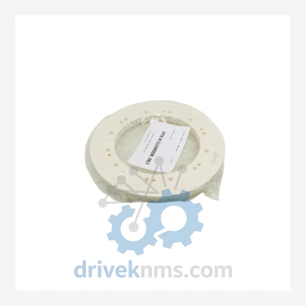
The upper electrode clamp ring (ceramic) referenced by part numbers 716-028028-004, VCC-15-B-R1, 311750-001, and 850B-23172 is a critical consumable within the C3520 TCP etch chamber. It functions as the mechanical retention and dielectric isolation interface between the upper electrode assembly and the chamber body. Ceramic construction provides resistance to plasma erosion, chemical attack from fluorine-based etch chemistries (CF4, CHF3, NF3), and thermal cycling stress. Dimensional tolerance and material purity directly affect process uniformity and particle performance.
The C3520 belongs to Lam Research's second-generation TCP (Transformer Coupled Plasma) etch platform lineage. The TCP architecture was introduced in the early 1990s as an inductively coupled plasma (ICP) source design, replacing earlier capacitively coupled systems to achieve higher plasma density at lower ion energies — a requirement for sub-micron feature etching without substrate damage.
The C3520 succeeded the earlier C2 and C3 chamber generations, incorporating a revised upper electrode geometry, improved RF matching network, and updated gas distribution ring design. It was optimized for 200mm wafer processing and supported a broad process window for oxide, nitride, and polysilicon etch. The chamber's modular construction — separating the source, process kit, and wafer handling subsystems — allowed incremental upgrades without full chamber replacement.
As the industry transitioned to 300mm wafers in the early 2000s, the C3520 platform entered a maintenance lifecycle phase. Lam Research's Flex and Kiyo series represent the current-generation successors for advanced node etch. However, C3520 chambers remain in active production at facilities running mature nodes (90nm–350nm), where capital equipment replacement is not economically justified. This has created a stable aftermarket for C3520 process kit components, RF components, and electromechanical assemblies.
The following part numbers represent verified components associated with the Lam Research C3520 TCP etch chamber platform. Parts are categorized by functional subsystem:
Upper Electrode & Source Assembly
Lower Electrode & ESC Assembly
Gas Distribution & Process Kit
RF & Power Delivery
Wafer Handling & Lift Pin Assembly
Lam Research's standard OEM support for the C3520 platform has been progressively reduced as the tool generation ages. Lead times for OEM-sourced consumables have extended, and certain part numbers have been formally discontinued. DriveKNMS maintains an independent inventory of C3520 process kit components, RF assemblies, and electromechanical parts sourced through authorized secondary market channels, decommissioned tool teardowns, and direct manufacturer relationships.
For facilities operating C3520 chambers beyond OEM support windows, DriveKNMS provides: verified cross-reference matching for superseded part numbers, access to new-old-stock (NOS) inventory for discontinued SKUs, and refurbished assemblies with documented test records. Procurement teams managing C3520 installed base are advised to maintain a minimum 6-month buffer stock for high-consumption consumables (upper electrode, focus ring, lift pins) given extended lead times in the current supply environment.
C3520 ceramic and quartz components undergo dimensional inspection against OEM engineering drawings using CMM (coordinate measuring machine) verification. Critical dimensions include electrode diameter tolerance (±0.1mm), clamp ring inner/outer diameter, and surface flatness. Material certification (Al2O3 purity for ceramic components, fused silica grade for quartz) is verified against supplier certificates of conformance.
RF assemblies (match networks, cable assemblies) are bench-tested for impedance characteristics, insulation resistance, and connector integrity prior to shipment. ESC assemblies are tested for chucking voltage response and leakage current. All refurbished assemblies are tagged with inspection records, technician ID, and test date. Components are packaged in ESD-safe, cleanroom-compatible packaging (Class 100 equivalent) with nitrogen purge for moisture-sensitive ceramic parts.
© 2026 DriveKNMS. All trademarks belong to their respective owners. Specifications are for reference only and subject to change without notice. Verify all parameters against official documentation before installation.
Related Paths
Sanken DK14256A Series: Comprehensive Module Range and Technical Overview The Sanken DK14256A is a purpose-built circuit board module deployed across…
KEB COMBIVERT F5 Series: Comprehensive Module Range and Technical Overview The KEB COMBIVERT F5 is a general-purpose AC variable frequency…
BIZERBA Printer Power Supply Series: Comprehensive Module Range and Technical Overview BIZERBA SE & Co. KG, headquartered in Balingen, Germany,…